
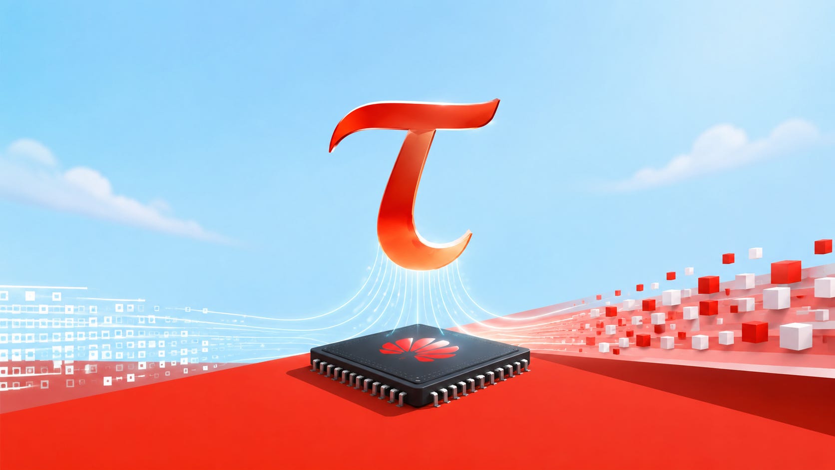
👀The Tau Law: Huawei Wants to Change the Rule of the Chip Race
It's more like a methodology for surviving the near term, for keeping Huawei’s silicon competitive for as long as EUV stays out of reach.

A week ago my dad called me with a joke. He said Huawei had just released a new semiconductor principle called 韬定律, the Tau Law. My first name is 君韬 (Juntao), and Tau 韬 sits right there in the middle of it. So by his logic, Huawei owes me a naming-rights fee. I told him I would settle for a Huawei Mate 80 smartphone.
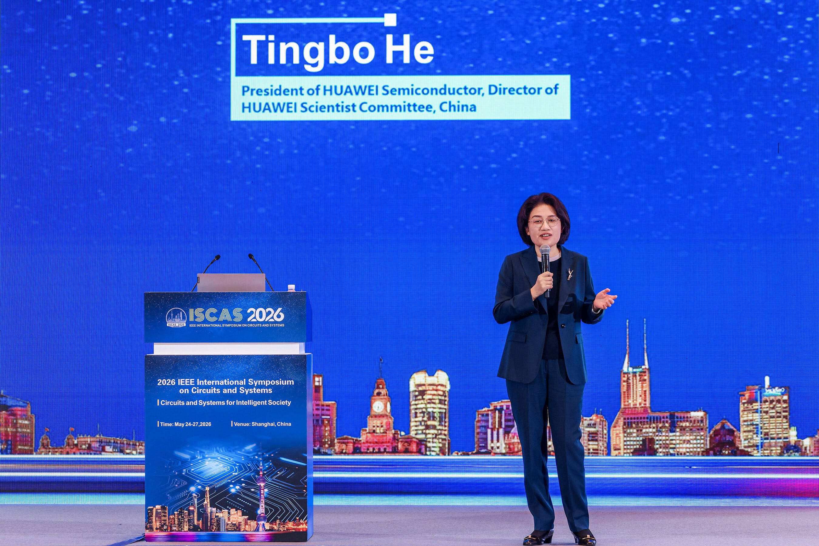
The Tau Law was first unveiled by He Tingbo, who leads Huawei’s semiconductor business, at the IEEE ISCAS conference in Shanghai on the morning of May 25. Huawei also released the paper A Time Scaling Theory for Multi-Layer Electronic Systems that further explains this principle.
I am not a chip expert, but I have written multiple stories about China’s AI silicon, from the outside looking in. So when a new study shows up wearing my own name, creating new buzz, and immediately starts moving stock prices, I want to understand what it actually is. Here is what I learned.
Personal update: Last week I launched Chinaidb.com, a one-stop intelligence source for China’s AI ecosystem, covering models, funding, applications, and news all in one place. I’d love for you to check it out and share your thoughts. Any feedback is greatly appreciated!
What is Tau Law

The core thesis is surprisingly simple. He Tingbo said Moore’s Law, the old rule of dimensional scaling, is slowing down beyond 7 nanometers, and the returns from simply making transistors smaller have flattened. So Huawei proposes a different yardstick. Instead of optimizing for size, optimize for time, the speed at which a signal travels through the whole electronic system, from a single device up to a gigawatt-scale AI data center.
That is where the name comes from. In physics and electrical engineering, τ (tau) is the standard symbol for the RC product, resistance times capacitance, which defines how long it takes a signal to propagate through a circuit.
Moore’s Law, named for Intel co-founder Gordon Moore, is the observation that the number of transistors on a chip doubles roughly every two years with little rise in cost. It was an empirical rule that hardened into an industry roadmap, and that roadmap is what powered the modern information age and nearly every device we touch. The computing power of today’s single integrated circuit is about 2 billion times what it was in 1960.
The catch is that you can only make things smaller until you can’t. Moore’s Law has been slowing for years. Former Intel CEO Pat Gelsinger has said the doubling now happens closer to every three years rather than every two, though he insisted Intel had strategies to claw the pace back. Huawei’s argument is that the industry needs a second engine for when the first one stalls. The Tau Law is its candidate.
Huawei’s Tau Law roadmap runs through 2031, and by then it claims to push past 400 million transistors per square millimeter, a density equivalent to a 1.4nm node. As Huawei does not have access to the lithography that the rest of the industry outside mainland China uses, the entire story is to explain how it intends to get there anyway.
One important difference from Moore’s Law: there is no universal rate like a doubling every two years across the board. Huawei predicts instead that under the Tau Law, performance improves at different annual rates depending on what the chip is for. It defines that annual improvement through a scaling factor it calls α (alpha):
Mobile devices: roughly 1.3x per year, the modest pace you would expect for power-constrained hardware.
Autonomous systems: roughly 1.5x per year for safety-critical applications.
AI workloads: up to 10x per year, because in this sector raw throughput converts almost directly into economic value.
Why Huawei, of all companies

Every company faces the slowdown of dimensional scaling. Huawei faces something much more severe, and the Tau Law cannot be understood without it.
In 2019 and 2020, Huawei and its chip-design arm HiSilicon were placed on the U.S. Entity List. The Foreign Direct Product Rule was then rewritten so that any foundry, TSMC and Samsung included, was blocked from manufacturing a Huawei-designed chip if that foundry used U.S.-origin software or equipment. The same wave cut off the EDA giants. Synopsys, Cadence, and Siemens could no longer ship Huawei software updates, patches, support, or new licenses.
In October 2022 and again in 2023, Washington widened the aperture from individual firms to the entire country, restricting China’s access to advanced AI accelerators and to the tools used to build them, and barring U.S. persons from supporting advanced chip production at certain Chinese fabs without a license.
The keystone of the whole structure is EUV. Through multilateral pressure on the Netherlands (ASML) and Japan, the U.S. choked off the export of extreme ultraviolet lithography machines, the only practical way to geometrically print sub-7nm transistors, along with the most advanced DUV immersion systems.

But the blockade did not stop development. Huawei plows north of 20% of its revenue back into R&D, and a large share of that money has gone into a single strategic question: how do you keep advancing semiconductors when you are locked out of the equipment everyone else uses to advance? The Tau Law is the answer to that question.
Keep reading with a 7-day free trial
Subscribe to Recode China AI to keep reading this post and get 7 days of free access to the full post archives.